Products
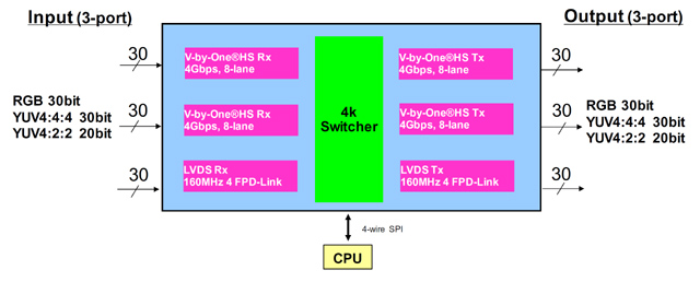
The IP00C251 is a 4K 3-channel Cross Point Switch LSI with built-in high-speed serial interfaces of V-by-One®HS/LVDS Tx and V-by-One®HS/LVDS Rx in one chip.
It can be used to connect high-speed image signals between multiple chips, including FPGAs, such as conversion between V-by-One®HS and LVDS and split/select image signals.
In addition, the built-in line buffer makes it possible to exchange images among three synchronized input images. Furthermore, it is also possible to perform overlay/chromakey processing on synchronized 3-channel input images and synthesize them into 1 channel.
Input (4K60Hz x3)
30-bit RGB/YUV4:4:4/ YUV4:2:0, 20-bit YUV4:2:2
@V-by-One®HS 4Gbps, 8-lane 2-port
@LVDS 160MHz x 4, FPD-Link, 1-port
4K60Hz input up to 3-port
Output (4K60Hz x3)
30-bit RGB/YUV4:4:4/ YUV4:2:0, 20-bit YUV4:2:2
@V-by-One®HS 4Gbps, 8-lane 2-port
@LVDS 160MHz x 4, FPD-Link, 1-port
4K60Hz input up to 3-port
3×3 Cross Point Switch for 4K60Hz
In/Output Image Size
-
Horizontal synchronization signal interval: 16,384 pixels
-
Effective horizontal image area: 2,176 pixels
Genlock function
Available for synchronization.
Resolution Conversion
Horizontal Scaling down: 6-symbol LUT, Coefficient ROM(64-set)
333Mpix/sec 4ch, support 4k60x2 images processing
Image Correction
Flip function
Overlay function
Alpha Blending
Chroma Key
CPU I/F
4-wire SPI
Power Supply
3.3V/2.5V/1.1V
Package
385-pin, BGA (0.8mm pitch),19mmx19mm
Block Diagram
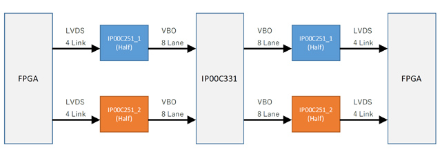
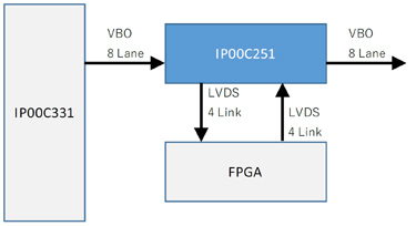
Application Samples [IP00C331 and FPGA I/F]
"V-by-One" is trademark of Thine Electronics, Inc.
